

ASML’s China “Risk”
(And the real bear cases)

If you are a long-time reader of Best Anchor Stocks, you’ll know that I’ve been following (and have owned) ASML for several years now. Throughout these years of owning ASML, I have encountered a primary and widespread bear case: it’s currently an EUV monopoly, but China will eventually figure it out. This bear case has been primarily parroted by two groups of market participants:
Those who don’t know much about ASML
Those who believe everything coming out of China (probably a subgroup of #1)
While I believe there’s merit to the claim that China will eventually figure out EUV (they most likely will), my goal with this article is to explain why I think the “WHEN” matters more than the “IF” when thinking about the investment thesis (and why the “WHEN” is still pretty far away). I’ll explain why I believe the risk is overblown and why people familiar with ASML typically give it little credit.
A good place to start is by claiming that I believe China will eventually figure out EUV. As Peter Wennink (ASML’s former CEO) used to say…
The laws of physics are no different in China than in the Netherlands.
Now, I am less optimistic that China will be able to bend the laws of physics like ASML has been able to do over the short to medium term because it takes much more than “throwing money at the problem” to come up with a credible competitor. Most people tend to focus on the “if,” but the “when” matters dearly in investing (every company is a 0 when looked at over a long enough investment horizon!). The passage of time without a low-NA EUV competitor has several important implications for ASML. First, the company will be able to improve the productivity of its systems, making it challenging for a potential competitor to undercut the company in price. The reason is that having a cheaper but far less productive system is unlikely to be great value for customers (more on this later).
Secondly, ASML is not standing still. Besides improving the productivity of its recently-launched high-NA system, ASML continues to work on the new generation: hyper-NA EUV. Even though hyper-NA is not expected this decade, ASML has shared that they are working on the technology and that the barrier thus far is one of cost (rather than technology). This is historically how ASML has operated: figure out the technology first (i.e., understand what’s possible), only to then lower the cost to drive adoption. They seem to be addressing the “cost problem” through tool commonality (albeit this is a topic for another article):
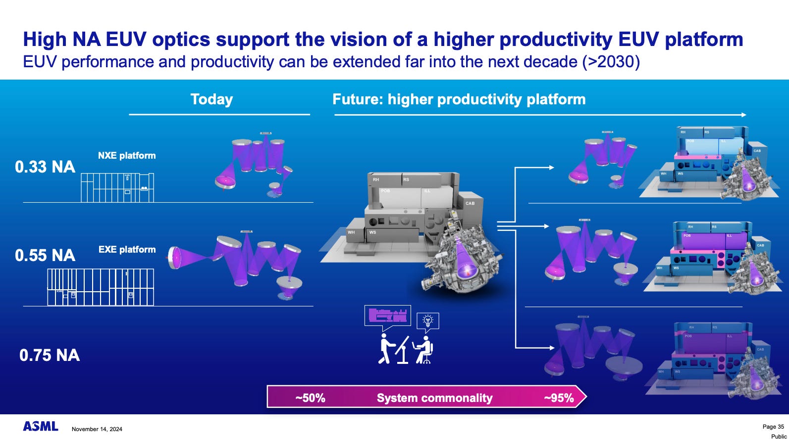
In short, the longer a credible EUV system takes to reach the market, the more ASML can leap forward. Many assume that ASML is waiting for someone to catch up, a notion that has not proven accurate with its DUV platform in the past. You have probably heard something like “China is 15 years behind EUV,” which leads many people to believe that in 15 years, China will be on par with ASML. The reality is that by 2040, China could be on par with the ASML of 2025.
Let’s discuss the “when” in more depth. I see several barriers to China figuring out EUV over the medium term (and even over the next 10+ years). The first barrier is the most obvious one to the ASML tourist: technological complexity. It’s no secret that EUV lithography is arguably the most complex technology on earth. ASML shared this week a video on the technology, which is well worth watching:
Manufacturing leading-edge chips (in their entirety, not just the lithography step) is also one of the most complex processes on earth. Testament to this is the fact that there’s only one company in the world capable of manufacturing EUV lithography systems (ASML) and (currently) only one company able to manufacture leading-edge logic chips at scale (TSMC). This is despite many investing billions over time to solve the same problem. The challenge seems quite hefty, but what makes it so complex? A couple of things.
First, one must bend the laws of physics to be able to print an atom-level pattern into a chip at scale. It’s not the atom-level part that makes it challenging (although it also does), but the fact that ASML’s EUV systems can print said patterns at a rate of +200 wafers per hour. This productivity ultimately enables cost-efficient manufacturing, which is key to continuing to power the mass adoption of technology. China conveniently leaves the cost part of the equation out of the announcements of domestically manufactured leading-edge chips (i.e., we all know that Huawei was able to manufacture a 7nm chip domestically, but we don’t know how much all the multi-patterning costs).
To make it even more challenging, ASML relies on a myriad of suppliers that make up one of the most complex supply chains on earth. It was only through this highly specialized (and exclusive) supply chain that ASML was able to bend the laws of physics. Some notable suppliers stand out. Two of the most critical components of an EUV system (the lens and the light source) are manufactured exclusively for ASML by Carl Zeiss and Cymer, respectively. ASML partly owns Carl Zeiss, whereas Cymer is wholly owned (acquired in 2013). Contrary to what many people think, Cymer’s light source was possible thanks to ASML (they did not outright buy a functioning EUV light source from the US).
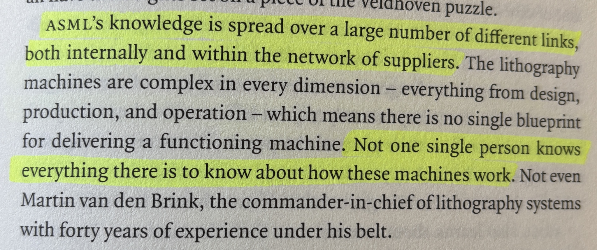
The complex supply chain and ASML’s role as an assembler within it mean that a copycat would not only have to mimic one company but also a highly complex supply chain. After the challenging task of mimicking said suppliers, the copycat would have to be able to assemble said components so that they work at scale. The book ‘Focus: The ASML Way’ explains that there’s not one single person at ASML who knows how an EUV system works:
Many will point out that we should never rule out China from mimicking a manufacturing process, and for good reason if history is any guide. China’s ambitions were met with similar skepticism in the automotive, smartphone, and solar panel industries, and the country has managed to partly/fully dominate these today. While I understand why people might feel tempted to draw comparisons with said industries, we are talking here about a far more complex process than China has ever attempted to copy. The playing ground is also different this time.
China leveraged Apple’s and Tesla’s decades-long expertise to develop domestic manufacturing capabilities for smartphones and EVs. This is simply not possible with lithography, as EUV shipments to China have been banned from the outset, and none of the critical parts of the supply chain were ever housed in China (it seems the West learned its lesson).
Despite not having the same tools at its disposal, China is trying to make progress. However, its developments over the years portray why the risk of China figuring out EUV is not a short- to medium-term risk. Goldman Sachs recently shared the following graph claiming that China is “at least” 20 years behind ASML’s leading-edge tech (EUV), or said differently: that China has not yet managed to come up with a credible immersion DUV system, which ASML manufactured more than a decade ago:
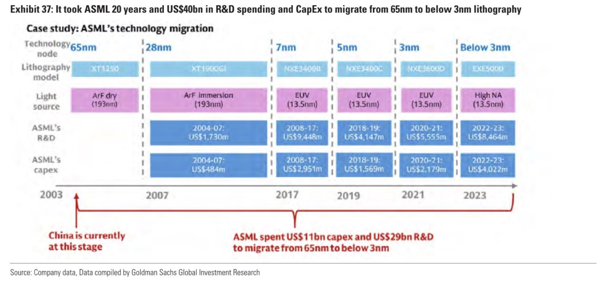
China’s ambition to dethrone ASML can be encapsulated in a company called SMEE (Shanghai Microelectronics Equipment). SMEE is the only domestic company in China that manufactures lithography equipment, and it has the backing of the CCP. But where does SMEE’s technology currently lie? Pretty far away from ASML’s decade-old technology.
In the graph above, Goldman Sachs portrays that SMEE’s most advanced machine lies somewhere in the 65nm node, but there have been some recent (albeit incomplete) news. In January 2025, SMEE unveiled its latest lithography system, capable of manufacturing at the 28nm node with a single exposure.
However, there’s a catch, one that China conveniently seems to overlook time and again: SMEE shared no performance metrics related to the new system (we don’t even know if it’s in high-volume manufacturing), meaning we can’t compare it to those of ASML. To add insult to injury, while SMEE claims that the system is domestically developed, there are reasonable doubts about whether all its components are domestically sourced (especially regarding the optics).
Still, if proven to work in High Volume Manufacturing (a big if), this system would most likely be far less productive than ASML’s NXT:1950i, which can print patterns on almost 300 wafers every hour. ASML introduced the NXT:1950i around 2008. If we assume that SMEE’s new 28nm technology works in HVM (for which there’s no proof), the company would be approximately 15 years behind ASML. Despite this, some people believe that SMEE is close to solving EUV because they have filed for a couple of patents. The “patent” argument is interesting because many believe it indicates that a system is nearing completion. The reality, however, is much different. ASML filed for its first EUV patents around 1999, but only released its first EUV system 18 years later!
While not entirely valid in the medium term, I believe there’s an argument for China eventually catching up to DUV technology. However, ASML is also protected to some extent from China’s encroachment in its DUV business. Part of the reason lies in yield. Many tend to believe that ASML is “doomed” if China develops DUV or EUV technology, but the reality is quite different.
One of the semiconductor industry’s north stars is yield. Yield measures the percentage of functional chips per wafer. The higher the yield, the more functional chips can be produced on a single wafer, and therefore the lower the manufacturing costs per chip. The topic of yield shifts what appears to be a question of price into a question of total cost of ownership. In short, it’s not only the cost of the systems but also how much I can make using the system over its lifetime. Let’s look at a quick example with EUV.
Let’s assume a 2nm wafer can host up to 80-90 GPU/AI chips (these are typically larger in size than standard CPUs). TSMC is expected to sell such a wafer for around $30,000 when it ramps production in 2025/2026. If we assume the yield is 100% (which it rarely is, especially during ramp), then the cost per die will be approximately $350 (midpoint). However, if the yield drops to 95%, then the cost per die suddenly increases to $371. Add this difference across many wafers, and the apparently minor differences in yield can result in substantial differences in cost. At $30k per wafer, one can also imagine that being able to churn more wafers per hour is a significant cost advantage (the foundry business is primarily a fixed-cost business). ASML’s systems carry a hefty price, but they also generate considerable value over their lifetime, and productivity and yield are key to this value creation.
Due to the hundreds of steps necessary to produce a sellable wafer, it’s tough to pinpoint precisely how much value ASML creates with its systems, but we can infer that the value added is pretty significant. At a price of $30,000 per wafer, an EUV system capable of single patterning 200 2nm wafers per hour will be playing a key role in enabling a lot of revenue for TSMC once those wafers are fully manufactured. Calculating how much is not easy task (due to leading edge chips requiring around 20-30 EUV layers inside a total of 80-100), but it does mean that there’s more to the story than the cost of the equipment. If a lithography system can churn out wafers at a significantly faster clip than a competing solution it will be much more valuable for its owner (more so considering that ASML’s systems never stop working and are installed for decades). In short, the driving force of the equation is not the initial price but rather the total cost of ownership, and there’s much more to the total cost of ownership than outright capability.
The key question here is…
What does China need to achieve similar productivity levels to those of ASML?
Besides having the capability (i.e., the raw technology), they would also need to curate said technology in high-volume manufacturing. This leads us to the chicken-and-egg problem. ASML has, over the years, been able to fine-tune its systems due to access to data from millions of wafer passes. This data collection has been possible because the equipment is embedded in its customers' high-volume manufacturing operations. Now, without access to HVM, you can’t have the data to fine-tune the equipment, but without this data, it’s pretty tough to get a foot in the door of high-volume manufacturing. A tough spot to be in, unless a customer decides to make an economically irrational decision. ASML is well aware that nothing prevents a customer from making an irrational decision, which is why it refrains from price gouging its customers despite its monopolist position. The objective is to create value and share it with the customer without giving the latter a reason to look for alternatives.
Despite ASML enjoying significant protective barriers, it’s also worth considering what might happen if China eventually succeeds. The first thing to note is that no domestic firms in China can access EUV technology, as the US banned exports from the outset. This means that ASML’s EUV China revenue is currently $0. This is not the case for DUV, something that I’ll discuss later.
The other thing that comes to mind is that foreign suppliers would unlikely be “allowed” or “willing” to use China-based EUV technology for geopolitical reasons. Note that China is known for stealing IP, and you would essentially be sharing both process and design IP with them by using their systems. China could also use this HVM data to develop better systems, something that I don’t think Western political leaders would appreciate.
With China not really being a bear case for ASML’s EUV technology, let’s take a look at what I consider to be the real bear cases for ASML.